What are 3D Printed Electronics? Let us tell you…
The complexity of electronics combined with the capabilities of 3D printing. Heard of 3D printed electronics but want to know more?

Kieron is a freelance writer and Digital Consultant who doesn't consider himself a design lover but a user of design - which to him is more than enough.
LinkedinDesignTech
Industrial
Plastic
The ability to 3D print electronics is making waves in an industry plagued by long stints of R&D and a never ending cycle of prototypes and new releases.
But what exactly does this process entail? And how, as a designer, architect, or artist, can it help you? Is it sustainable? What are the dangers? And what should you know about it?
This guide is a useful starting point for you to find out…

What is it?
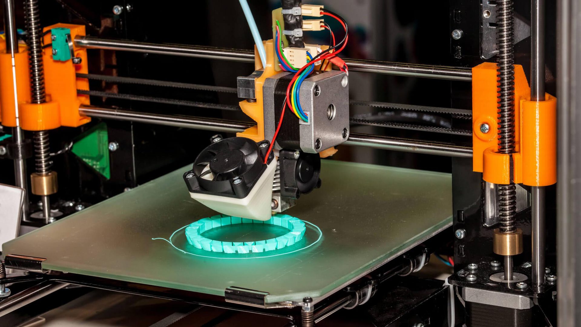
3D Printing objects with electronic functionality is a relatively new concept.
It involves the use of material jetting technology, which is used to jet conductive and insulating inks onto the printing surface.
These inks are applied in lines as thin as a few microns before UV light is used to solidify the inks.
The use of material jetting facilitates multi-material 3D printing, which is particularly useful for the electronics industry.
This means that the different elements necessary in electronics, such as functional circuitry and enclosures, can be manufactured in a single print run.

What materials are used when 3D printing electronics?
Where systems could typically use just one material in the 3D printing process, recent advancements have enabled the involvement of multiple materials.
This allows manufacturers to merge conductive materials with non-conductive materials.
The thermoplastics used in the 3D printing process are often made with copper, carbon and graphene.
Meanwhile, proprietary conductive and dielectric inks are used simultaneously to build functional circuits and antennas. This expands the range of functions in 3D printed electronics.
Because the process combines multiple materials into the same 3D object it also requires a solvent to ensure their compatibility. The particular solvent used is known as an orthogonal solvent, which is specifically designed not to cause damage to the different components.

What can 3D printing electronics produce?
With 3D printing electronics, it is possible to make various types of boards that can be programmed and connected to prototypes.
A very wide range of inks can be utilized enabling a full range of printed electronics functionality: conductors, semiconductors, dielectrics, resistors and more.
The process can be used to manufacture electronic components such as resistors, capacitors, antennas, sensors, and thin film transistors.
Using the 3D printing process, it is also possible to rapidly 3D print fully functional electronic circuits that contain electrically-conductive metallic inks and insulating polymeric inks, which could be useful for medical devices, radio frequency shielding surfaces and novel structures for harvesting solar energy.
Today, however, it’s main applications include printing electronics for use in prototypes for upcoming products, prosthetics and more complexly shaped electronic products.
Give me a step-by-step
While several methods exist for 3D printing electronic components, they typically mirror the various steps utilised in regular 3D printing. The main difference is the use of a dual-material fused filament process with conductive thermoplastic filaments.
As with all 3D printing, a digital CAD model of the desired part is designed, which serves as the printer’s instruction model.
When the printing process begins, a trace or “fingerprint” is created, and then the requisite materials needed for that specific part are added in layers.

What machinery is used when 3D printing electronics?
Specialised machinery is required which integrates a precise inkjet deposition printer with dedicated nano-inks and software capable of printing electronic circuits such as printed circuit boards (PCBs), antennas, capacitors and sensors.
Can I do it at home?
Due to the complexity of the process, it is not possible to replicate it at home unless you have the capability of manufacturing your own 3D printer.
With the relevant machinery, it is possible to 3D print electronics at home.
Find out more about manufacturing processes, don’t miss What is Explosive Forming? Let us tell you…

What are the pros & cons of 3D printed electronics?
At the core of every electronic device is a Printed Circuit Board (PCB) which is difficult to produce. Luckily, with the advent of 3D printing, manufacturing these circuit boards is less challenging.
The benefits of 3D printing electronics range from faster time-to-market, greater freedom of design and customisation.
This is because with the advent of 3D printing electronics manufacturers can create prototypes of circuits and circuit birds in-house, reducing procurement expenses and eliminating concerns about IP infringement.
3D printing also opens up opportunities to design complex shapes and components. For example, multilayer circuits can now be 3D printed on non-flat, flexible surfaces, which would not be possible with traditional manufacturing techniques.
Components can also be printed onto 3D surfaces eliminating the need for a separate substrate and reducing the size, thickness and weight of the end product.
However, there are several limitations when it comes to 3D printing electronics, not only because it is limited in the types of parts it can produce.
Whilst the recyclability of 3D printed electronics is an area being explored by various researchers, it remains a con due to what is currently possible.
Another downside to 3D printed electronics, and in fact, all 3D printed products is their structural integrity.
Whilst printed layers adhere together in some cases, and under certain stresses or conditions, they can delaminate.
Another major downside to 3D printing as a whole is its increasing popularity and accessibility. On one hand, it democratises the manufacturing processes but it also makes it easier to fake and counterfeit products.
I want to know if it’s sustainable…
Whilst 3D printing electronics can minimise the manufacturing footprint by localising production, the difficulty in recycling the various components means it can’t be considered a sustainable process.
I want to know more!
There are several resources that are useful when it comes to building your knowledge around 3D printed electronics.
If you want to learn more check these out:
- A visual demonstration of the 3D printing process used to manufacture electronics.
- An explanation of the various capabilities of 3D printing electronics.
- A paper detailing the evolution of 3D printing electronics.
- A breakdown of the various benefits and current systems employed when 3D printing electronics
- A detailed research into the future of 3D printing electronics and its benefits when used for prototyping.
Fascinated by 3d printing? Don’t miss 3D printing ceramics: Interview with Hilda Nilsson.